


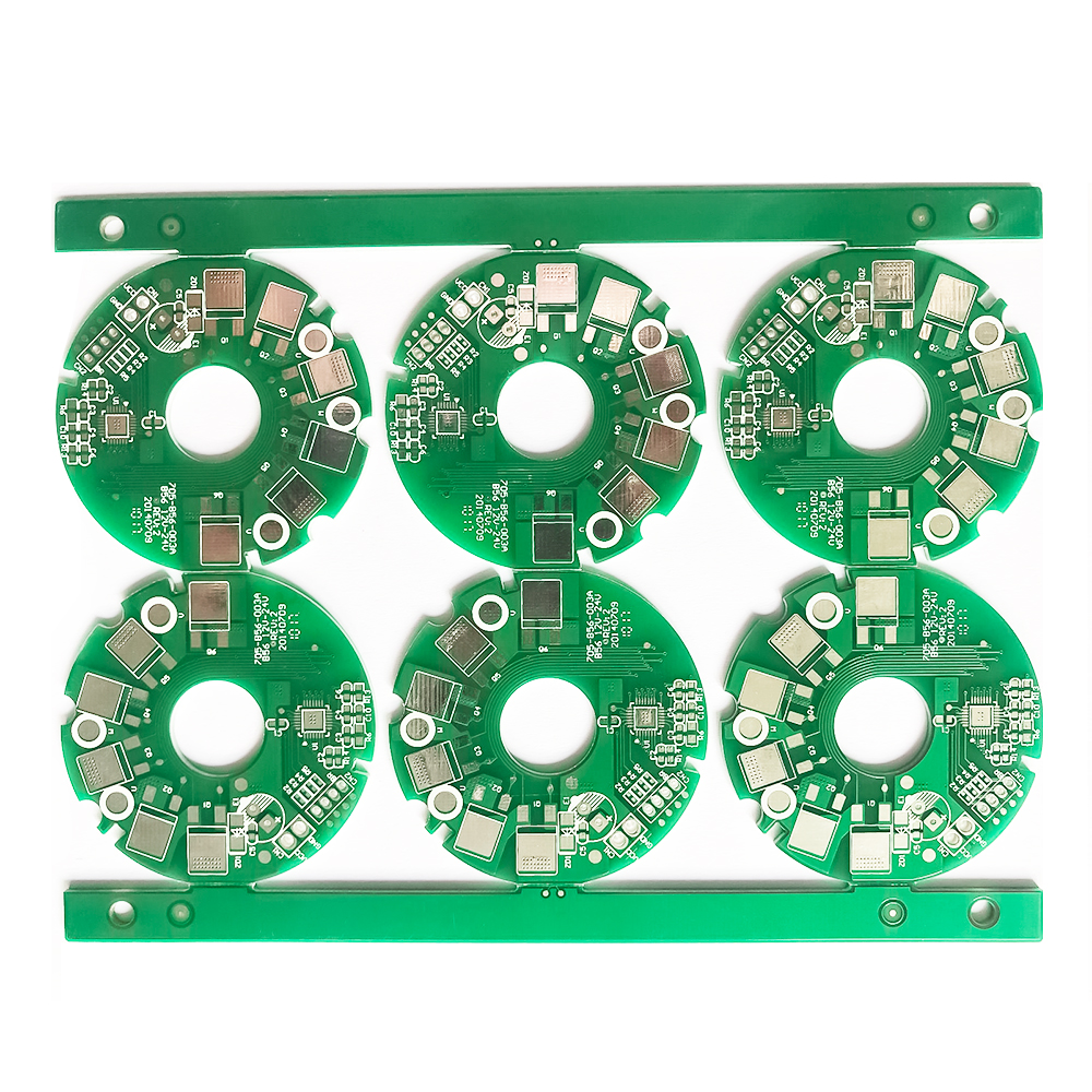
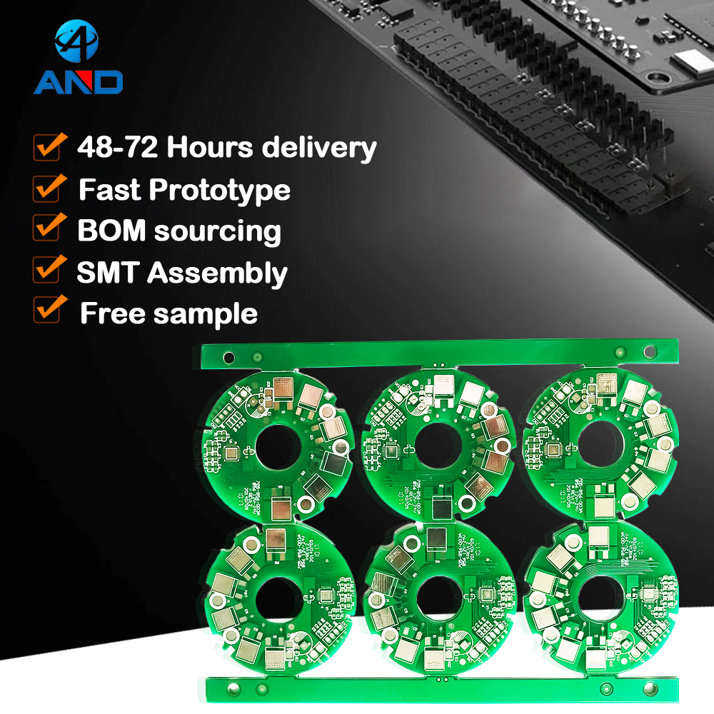
Two Layers Pcb Oem Service Copper Base Osp Double Sides Mcpcb
Product Overview
selects high-quality species to carefully plant Two Layers Pcb Oem Service Copper Base Osp Double Sides Mcpcb based on scientific planting methods. It is green, pollution-free, safe, and healthy. Two Layers Pcb Oem Service Copper Base Osp Double Sides Mcpcb is excellent in outlook as you can see by pictures. The product can serve as an easily noticeable landmark. Its giant shape, bright colors, and customized logo can provide location information for people lost in the crowd. Two Layers Pcb Oem Service Copper Base Osp Double Sides Mcpcb is widely applicable to the cutting and deep processing of industrial materials in the following fields: decoration, aerospace, electricity, new energy, chemical industry, automotive manufacturing, and others. The product is easy to use. Instead of having phone owners hovering around the complicated instruction, this newly designed product features high user friendless.
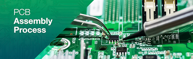
Step 1: Solder Paste Stenciling

Step 2: Pick and Place
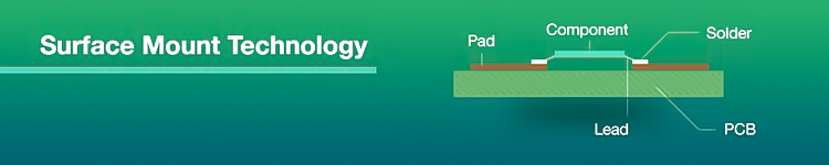
Step 3: Reflow Soldering

Step 4: Inspection and Quality Control

Step 5: Through-Hole Component Insertion
Step 6: Final Inspection and Functional Test
Company Introduction
Situated in is mainly engaged in the development, production, processing, and sales of redefined our own development direction and product positioning by exploring the new economic growth points and new market demand. Under the guidance of development direction, we created the brand based on unremitting efforts and exploration. firmly believes that high-quality products and services serve as the foundation of customer's trust. A comprehensive service system and a professional customer service team are established based on that. We are dedicated to solving problems for customers and meeting their demands as much as possible. Excellent in production technology and friendly in service attitude, ranks top in the industry for the comprehensive business power. We have experience in providing custom services of different products for multi companies. All these gain us a wide reputation in the industry.
Dear customer, thanks for your interest in this site! If you have any questions about our products, please dial our consulting hotline. is pleased to serve you!
